JTAG FLASH Programming
FLASH memory is a flexible storage solution for CPU and micro-controller based designs. Programming FLASH devices in or out of the system can be done using one of several techniques. Determining the optimal technique is often a challenge; a designer must develop a solution that balances flexibility, cost and programming time.
Programming FLASH using IEEE 1149.1 JTAG
IEEE 1149.1/JTAG enables in-system FLASH programming without requiring expensive in-circuit test equipment (ICT) or the addition of test access points to the PCB. Programming with 1149.1 facilitates the use of a common tool and programming methodology for design verification and debug, manufacturing test and field changes.
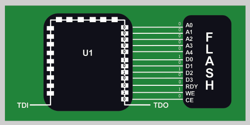
A FLASH device is programmed in-system by scanning the address and program data to the proper scan pins of an IEEE 1149.1 boundary-scan device that is connected to the FLASH memory. At the appropriate time, the CE and WE pins are pulsed and a location in the FLASH memory is programmed. This sequence is repeated until the device is fully programmed.
 FLASH Programming Using The Eclipse Family
Unlike some JTAG 1149.1 software packages, FLASH-programming support is a standard feature in the Eclipse family. Devices can be programmed with the Eclipse Test Development Environment or with the Scan Executive Manufacturing Test Station.
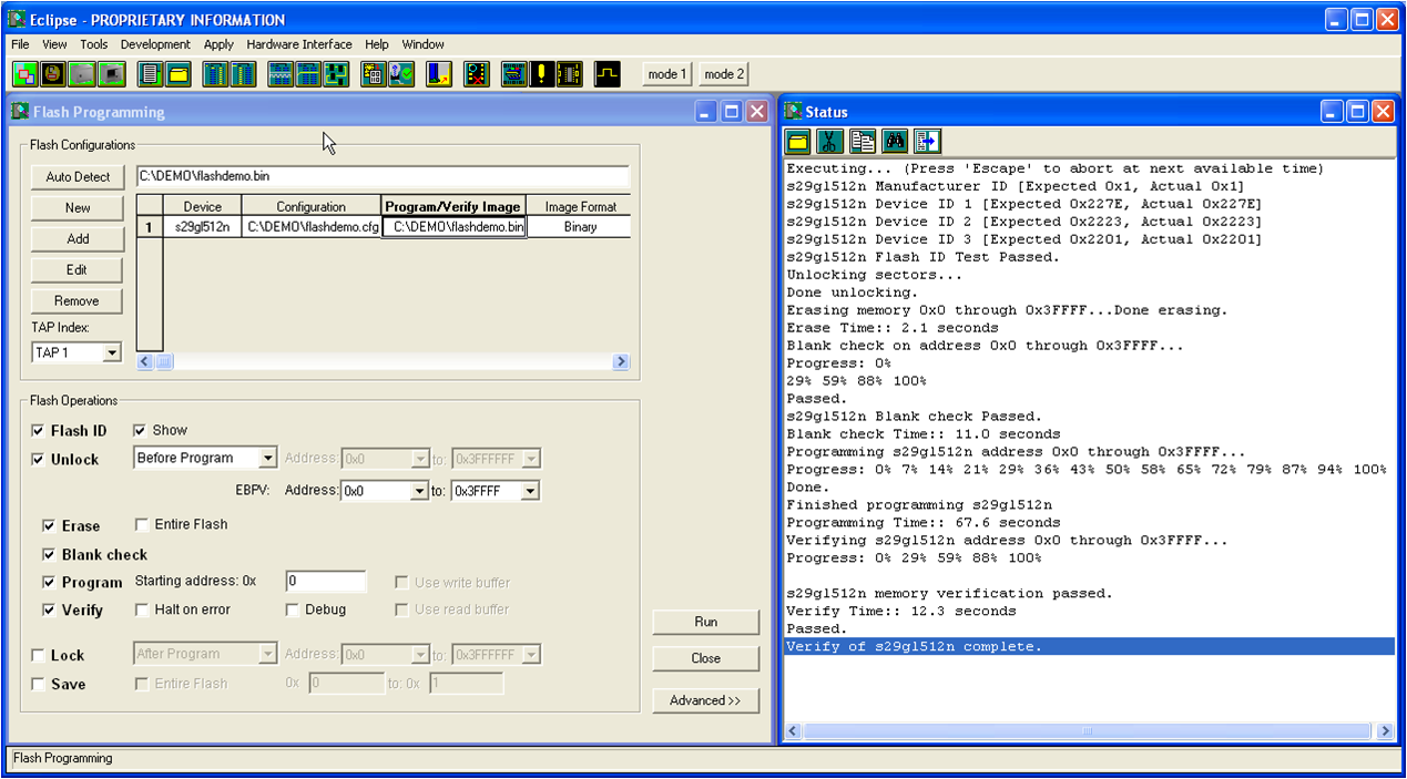
Programming FLASH with Eclipse is a straightforward operation. The user selects a FLASH device model from the Eclipse memory library and supplies the FLASH image to Eclipse. The software automatically sequences the FLASH data so the device can be programmed and verified. Optionally, a user may setup a repeatable flow using predefined FLASH programming functions in the Eclipse TCL/TK scripting langauge.

Flash Programming White Paper
Fast Flash Programming with FAC Whitepaper
Standard Eclipse FLASH Programming Features
- No special software package or additional emulation tool is required,
both the Eclipse Test Development Environment and the Scan
Executive Manufacturing Test Station support in-system JTAG FLASH
programming
- Fully predictable programming times using the
UltraTAPTM Intelligent Test
Controller (# of bits in the scan-chain * TCK period * number of
scans needed for a write operation * number of locations to
program)
- Fully predictable read times using the
UltraTAPTM Intelligent Test
Controller (# of bits in the scan-chain * TCK period * number of
scans needed for a read operation * number of locations
to read)
- Large library of memory models including Intel and AMD FLASH parts
- Easy creation of custom memory models without C++ coding
- Automatic reading/verifying for S-Record, Intel Hex and binary COFF files
- No user intervention is required to fill don't care scan bits during FLASH programming
- User control of busses, tri-states, and non-1149.1 devices during FLASH programming
- Testing of programming path to FLASH before program sequence begins
- Automated checking of FLASH IDs before programming.
- Optional use of Xilinx USB Cable pod for programming
-
Need FLASH programming as fast as off-board FLASH programming?
Learn about the patented FAC here: Faster JTAG Flash programming
|


