Patented Technology
The UltraTAP® uses US Patent #6,594,802 and world-wide patents-pending to provide the undisputed industry's fastest on-board FLASH programming. With the UltraTAP® FLASH devices can be programmed and verified on-board at speeds in excess of 1.5Megabits per second (Intel StrataFLASH 28F128K3C).
Many vendors claim to support high test clock rates but their actual data throughput is limited by the amount of time it takes their software to determine failing/working bits. Intellitech's throughput does not stop at the PCB. The UltraTAP® throughput can be achieved regardless of the size of your PCB or multi-PCB System when used with Intellitech TEST-IP products. Routing TCK and TMS for operation above 20Mhz requires important design considerations. While some vendors may claim a 1149.1 POD speed of 50Mhz, they offer no additional on-board hardware such as scan-chain buffers and linkers that enable you to attain the higher speeds when the signals are routed on the UUT. Using the UltraTAP® and the Intellitech SRL, customers routinely run 40Mhz speeds on their PCB without impacting the design schedule to add buffers and voltage translators on board.
The UltraTAP® works seamlessly with all of Intellitech's IP and IC products for routing scan-chains and programming FLASH.
PCI, cPCI, PXI, Ethernet and PCMCIA JTAG interfaces
UltraTAP® is available with industry standard interfaces for PCI, cPCI, PXI, TCP/IP Network and PCMCIA. The same UltraTAP® pod can be used in all four of these environments. Fast throughput is essential when using the IEEE 1149.1 test bus to configure large FPGAs or program FLASH memory.
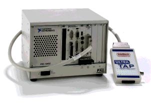 |
UltraTAP with PXI Interface Card (Shown in PXI Chassis. PXI chassis sold seperately from National Instruments) |
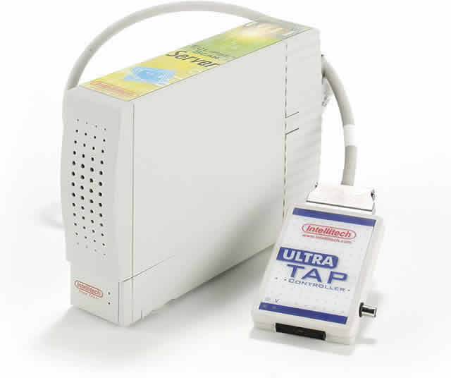
| UltraTAP with Scan Server TCPIP/Ethernet Interface . |
 |
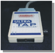
UltraTAP JTAG/1149.1 Features
|