Boundary Scan Test Development Software using IEEE 1149.x
The Eclipse Boundary Scan Test Development System is a
Complete Solution for Test, Debug and In-System Configuration of PCBs with Boundary-Scan, SPI, I2C and other standardized serial interfaces. |
 |
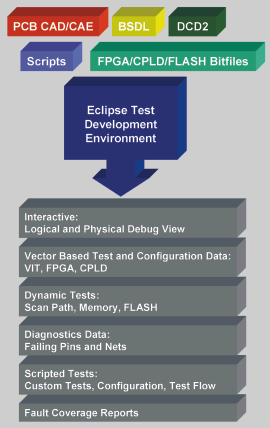
Intellitech's Boundary Scan software is called the Eclipse Test
Development Environment. The Eclipse TDE is part of a holistic solution that provides all
the features that are required to test real world printed circuit boards. This including important essential capabilities such as
boundary scan 1149.1 IC to IC interconnect testing, 1149.6 SERDES testing, memory interconnect testing, voltage testing of DC/DC converters and LDOs, i2c tests, SPI device tests, on-board FLASH programming, in-system programming for FPGAs, CPLD programming, schematic based debugging,
robust
pin level diagnostics, open-source JTAG scan scripting, LabView/TestStand VIs and built-in PXI/VXI/GPIB instrument support.
Eclipse scales to any size design
that conforms to the JTAG/1149.1 standard. Have a small PCB with a few BGA devices? Prices start at US$1595.00 for an Eclipse "small PCB" TDE license.
The Eclipse TDE provides engineers with a comprehensive set of
powerful tools that they can use to bring up and debug new designs
as well as create, validate and apply IEEE 1149.1 based configuration and test suites.
|
|
Quality and reliability are important factors in our new line of
optical networking equipment. We looked at a number of 1149.1 based test tools
on the market and we chose Intellitech as it had the most comprehensive
solution
|
|
|
Pete Marconi
VP of Systems Engineering
Axiowave Networks
|

|
Eclipse reduces
test development time
by capturing more design attributes
Eclipse accepts industry standard data
supplied by major CAE/CAD systems, IEEE 1149.1 BSDL
files and PLD configuration file formats from all
programmable semiconductor vendors so you can start debugging a
prototype in just minutes instead of days. With other IEEE
1149.1 tools much of the test engineer's time is spent re-entering
design information through proprietary GUIs, creating
'characteristic' models for non-JTAG devices or describing
PCB level busses in
proprietary Heirarchical description languages. "Demos" of some JTAG tools
may look a little like what Eclipse has to offer, but, the novice is not seeing the time the vendor spent manually creating and massaging input data to get the results in the demo.
|
|
"High quality board and system test, and effective board and system debug, are essential in ensuring the reliability and availability of Sun Microsystem's products. Intellitech's Eclipse and scan-based test is critical to meeting this goal. Sun has used, and is continuing to use, Eclipse on products ranging from processor modules to Enterprise servers. We have found Eclipse from Intellitech to be a flexible, cost effective test solution, which is deployed throughout Sun Microsystems as a part of Sun's test process."
|
|
|
Scott Davidson
Manager DFT Technology
Sun Microsystems
|

|
CAD/CAE Data Flow Diagram for Scan Test Development
Boundary Scan - Learn more about PCB test "constraints" and other features
Advanced Feature Set
- Patented interface to embedded SystemBIST configuration and test processor.
- Patented Concurrent JTAG test for testing multiple UUTs simultaneously
- Patented on-board JTAG FLASH programming as fast as off-board programmers
- Exclusive Logical Design Viewer and Pin toggle debugger based on your schematic
- Industry's easiest interconnect test generation flow with high fault coveage
- Hierarchical interconnect testing of multi-PCB systems
- Automated Memory Interconnect testing with hundreds of proven DDR/SDRAM/SRAM models
- Fast configuration of CPLD and FPGA
devices
- Industry Standard open scripting language - no proprietary limited languages
- Customize Eclipse using scriptinga language - add your own capabilities
- Netlist based constraints eliminates manual entry of 'Hierarchical description languages'
- Easy Integration to Other Design and Test Tools
|