|

Speed Flash Programming and Memory Testing with the Fast Access ControllerTM
FAC Overview
If you are looking for
traditional EXTEST based FLASH programming using boundary-scan
please see information at Boundary Scan based FLASH programming
The FAC is a plug-and-play IP
solution for processor (Micro-controller, DSP or CPU), FPGA Users and ASIC/SoC
designers who need to respond to customer demands for better
Design-for-Test and improved support for programming external FLASH
in a production environment. The Fast Access Controller is covered by
US Patent #6,594,802 and Canada patent #2404059 "Method and Apparatus for optimized access to circuits
for debug, programming and test". Asian and European
patents are applied for and pending. Intellitech's patented technology delivers the world's fastest
on-board FLASH and non-volatile memory programming. There is no need to perform stand-alone or in-line
device programming in order to achieve the optimum programming speeds.
On-Board Fast FLASH programming
The FAC IP achieves its fast on-board FLASH programming times by using advanced data de-serialization and protocol optimization algorithms to minimize the number of scan operations and data required during FLASH programming. This enables the FAC to program FLASH devices in-system over the standard 1149.1 bus at speeds equivalent to off-board programming. The FLASH memory protocols of the FAC are fully configurable in-system, using Intellitech's EclipseTM family of 1149.1 based tools allowing it to support a wide variety of FLASH memory devices and protocols from vendors such as Numonyx, Samsung, Toshiba, Sony, Intel and AMD.
The FAC IP can also be embedded
into an FPGA so it is an attractive alternative for PCB designers
who are under pressure from their test engineering groups to provide
direct physical access points for FLASH memory devices so
manufacturing can realize shorter programming times. It is also
useful for FPGA based PCBs that use on-board FLASH as a method of
storing FPGA configuration data. The FAC enables the IEEE 1149.1 bus
to be used as a central high-speed serial bus for in-system
configuration of all on-board FLASH devices.
If you are using FPGAs, you may already be using the FAC IP in one form. Xilinx and Lattice have licensed Intellitech's '802 patent (and foreign counterparts CA2404059, FR EP 1275183, GER EP 1275183, UK EP 1275183, NL EP 1275183, and HK 1052586) and Altera is a licensee of Intellitech’s flash programming technology.
This enables them to program SPI and NOR flash connected to an FPGA with the FPGA's bitstream.
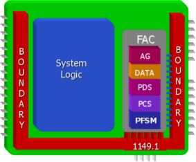 IC with Embedded FAC Blocks
AG - Address Generator
DATA - Data register 8 or 16bits
PDS - Programmable Data Sequencer
PCS - Programmable Control Sequencer
PFSM - Programmable 1149.1 State
Machine |
FLASH Memory usage and density is growing
The Cahners In-Stat Group forecasts that flash memory shipments will grow to $16 billion in 2004. This growing use of FLASH memory coupled with today's requirement to reduce manufacturing test costs is forcing product development teams to re-examine their current method of programming FLASH memories in order to find a faster, more flexible and cost effective approach.
Considerations when using FLASH devices in a system
- Changing customer needs or bugs often necessitate that system firmware be changed in the FLASH memory during a product's life cycle.
- In many cases, developments costs have replaced time-to-market as the major consideration a design team must address when building new products.
- Short programming times are essential as FLASH devices become larger and more prevalent.
- Methodology reuse is essential; a
successful in-system FLASH programming strategy must be able to be
deployed on multiple projects and support FLASH changes during
prototyping, manufacturing and in-the-field updates.
Drawbacks with current FLASH programming methods
There are many ways to program FLASH memory (stand-alone programmers, in-line programmers, in-circuit emulation ICE/BDM equipment, In-circuit "pogo-pin" testers, and boundary-scan testers), each method has certain drawbacks such as high cost and slow FLASH programming times. Each method is also a point solution targeted for only one phase of the product's life cycle. For instance, in-line programmers cannot easily be used during engineering prototyping and ICE/BDM equipment cannot readily be used in production test. If a system is being designed to enable remote software and FPGA logic updates, yet, another solution must be devised to allow each individual FLASH to be updated when the product is in the field. In some cases, 3 or 4 of these programming methods are required, each one costing more in equipment and engineering resources to support programming during each phase of the product's life cycle.
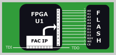 FAC loaded in FPGA and connected to external FLASH Device
Benefits of the FAC FLASH Programming Patented Technology
Enables in-system FLASH programming
The FAC is easily embedded into a design to enable and simplify in-system FLASH programming to accommodate firmware changes during any stage of a products life cycle.
Reduces the cost of FLASH programming throughout a product's entire lifecycle
The FAC is significantly more cost-effective
when
compared to methods that use external equipment to program FLASH devices. FAC has very limited impact on the design flow and does not necessitate a capital expenditure for dedicated or inline FLASH programming equipment.
Fast in-system programming
In-system FLASH programming using the FAC can be done in the same amount of time it takes to program a device out of system using expensive capital equipment.
FAC is scalable and reusable methodology
FAC is a proven plug-and-play IP solution
that can be used on multiple projects (processor, SoC, ASIC or FPGA)
|