Embedded Test Bus Solution- Not a JTAG Controller
Problem
Conventional methods for testing electronic
systems are being challenged to keep up with the increasing
complexity and cost constraints of today' s products. Current test
strategies often employ In-Circuit Test (ICT) equipment to test
subassemblies and in-house developed functional programs to test
integrated systems.
|
|
Intellitechs embedded test solutions provide us with a code-less
method to implement embedded test and re-configuration that lowers our overall
system cost.
|
|
|
Pete Marconi
VP of Systems Engineering
Axiowave Networks
|

|
Challenges testing subassemblies (PCB) with ICT
- Limited physical access on PCB with surface-mount parts and ball-grid array packaging
- Signal-integrity problems when high-speed 1149.1 tests are run on structures like SERDES connections using an bed of nails fixtures (Pogo Pins act as little antennas and degrade high-speed signals)
- Lack of scalability and the inability to re-use manufacturing test programs that were developed for ICT
- Increasing amount of configuration and
programming that needs to be done (in-system FLASH programming,
in-system FPGA/CPLD configuration) which drives up the time a PCB
is on ICT
Challenges testing integrated systems with functional test programs
- Functional test programs are ad-hoc/custom embedded software applications
- Functional test programs do not deterministically measure fault coverage
- High cost involved in developing and maintaining functional test programs
- Functional test programs normally require
a working system and offer limited value in system-bring up
Embedded Configuration and Test Solution - more than a JTAG Controller
|
|
Boundary scan is the platform on which board-level BIST will be built. BIST can potentially do for functional test what in-circuit test did for the old instrument-level production electrical test. Given the exponentially increasing complexity of boards, there will come a time when, if you don't have BIST, you won't be able to debug future boards at all.
|
|
|
|
Dr. Kenneth P. Parker and Dan Zimmerle, Agilent Technologies
Article in EP&P, 7/1/2002
|
The ideal solution provides the design and test engineer with a scalable and reusable methodology that augments existing test methods but supports anytime/anywhere testing and in-the-field re-configuration an entire system.
To implement this methodology Intellitech provides the TEST-IPTM family of patent-pending Infrastructure Intellectual Property (IP) modules.
Intellitech's embedded configuration and test solution augments ICT such that structural digital test can be done in-system and ICT can be better leveraged for analog testing
- Embedded Test eliminates the need for physical access
- Embedded Test supports in-system at-speed intereconnect testing without signal-integrity problems
- Embedded Test is completely scalable and reusable at any level of integration
- No software development or integration
needs to be performed as with low level "JTAG Controllers"
Embedded Test can enhance and reduce the dependence on functional test programs.
- Embedded Test can be built directly into the system and be run anytime and anywhere
- Embedded Test provides deterministic fault coverage
- Embedded Test is very cost-effective and can be reused at anytime during a product's life cycle
- Creating and validating embedded tests is
an automated process and does not require a working system
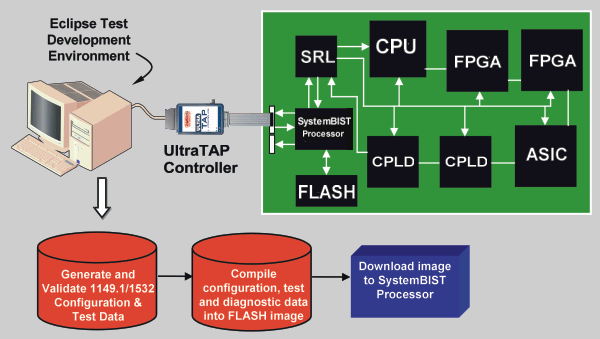
Intellitech's SystemBISTTM Embedded Configuration and Test Processor enables manufacturing tests (PCB and PCB to PCB) and device configuration suites to be developed, validated and embedded directly into the system. Embedded Test eliminates the need to run digital tests and device configuration using ICT. Embedded Test also permits the same set of tests to be used in lab prototyping, volume PCB manufacturing, System Integration, HALT/HASS tests, at customer power-up, field service and depot repair. System re-configuration could take place anywhere so that engineering changes could be easily made at any point in time during a product's life cycle.
In-system FLASH programming can be done using Intellitech's FAC IP. FAC achieves its fast on-board programming times by using advanced data de-serialization and protocol optimization algorithms to minimize the number of scan operations and data required during FLASH programming. This enables the FAC to program FLASH devices in-system over the standard 1149.1 bus at speeds equivalent to off-board programming. The FLASH memory protocols of the FAC are fully configurable in-system, using Intellitech's Eclipse family of 1149.1 based tools allow it to support a wide variety of FLASH memory devices and protocols from vendors such as Intel and AMD.
|